Open the layout view of the Resistive_divider cell and then copy/paste (Ctrl+C/Ctrl+V) an additional resistor.
Running a DRC (pressing F5) on the above layout results in the following error.
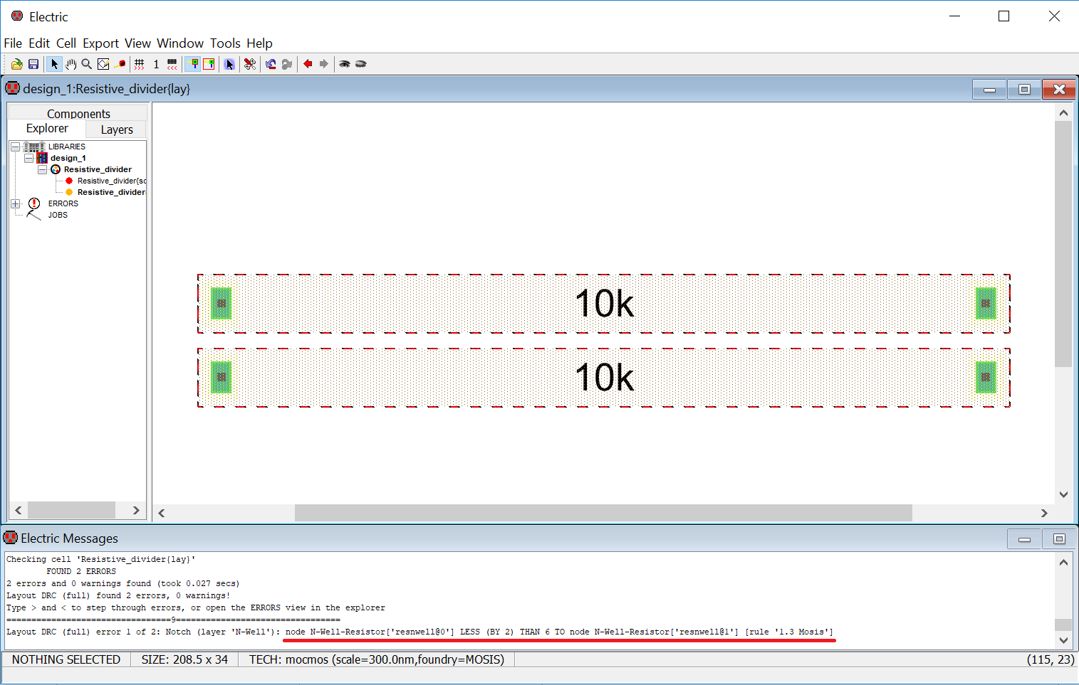
By pressing > we see that there is too little space between the N-wells.
Move the Nodes apart until the layout passes the DRCs. Of-course the error will not appear if you have initially placed both the resistors apart enough, which would satisfy the MOSIS rule for space between N-wells.
Then left click on the right port of the top Node and right click on the right port of the bottom resistor node. This will establish a metal1 Arc connection between the two resistors.
 Note that when you RIGHT click to connect the node, you have to be over the right side of the highlight box else you won’t connect the two ports and the resistor will fail DRCs (you will generate an Arc that isn’t connected).
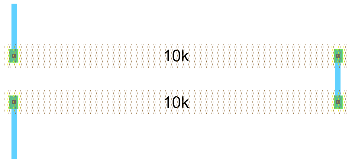
Connect a couple of more Arcs to complete the connections as shown in the figure in right.
Run the DRC to ensure there is no error.
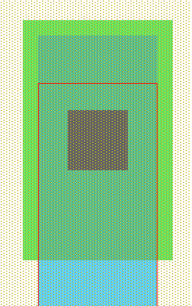
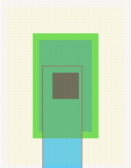 If we will zoom-in the N-well resistor and metal1 connection, we will find that there is a mismatch as shown in the figure. (Though this will not give you a DRC error if the minimum width of metal1 is achieved)
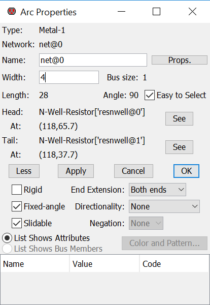
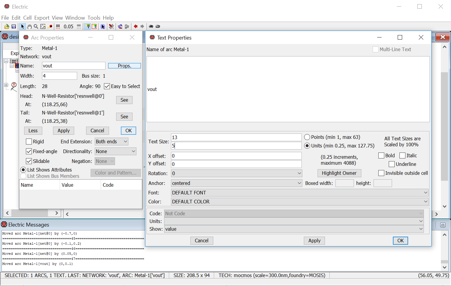
To match the width of the metal1 Arc with the connection to the N-Well resistor, we will increase its width by going to its object property (select the Arc and press Ctrl+I).
In the Arc Properties, change the Width to 4 as shown below.
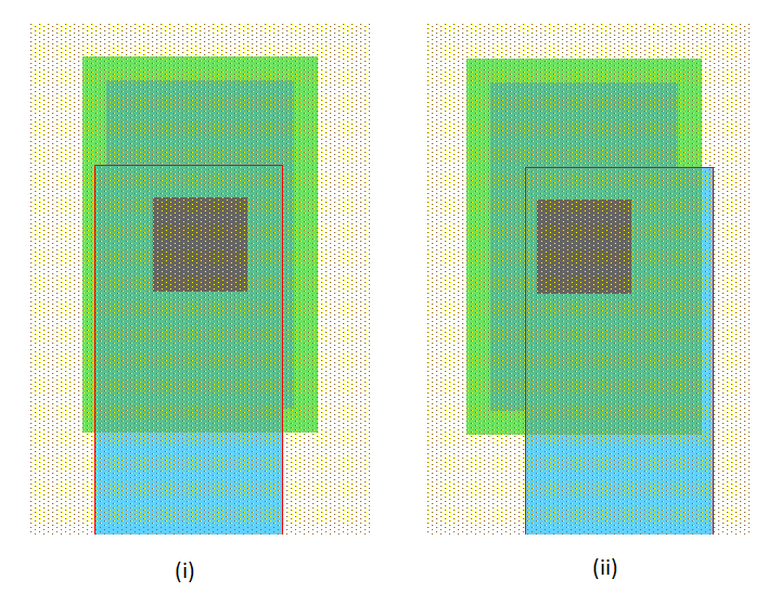
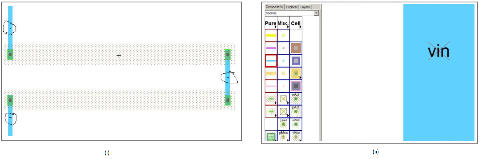
Now the width of the metal1 and N-Well are same. But both are misaligned as shown in the figure (i) below. When I move the Arc by selecting it and dragging it towards right through mouse, it shifts more than I wanted to, as shown in the figure (ii) below.
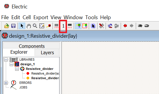
This happens due to the Grid Alignment set at 1 as shown in the below figure with a red rectangular box. So, whenever we tray to move anything, it moves for 1 major grid (10 minor grids).
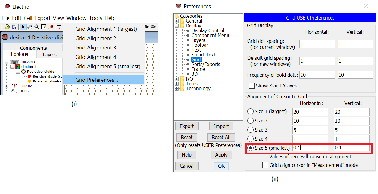
To change this to a lower value, click on it and go to Grid Preference as shown in the below figure (i). In the preference, change the Size 5 (smallest) to 0.1 as shown in a red rectangular box in the below figure (ii). This will help us to move any object horizontally or vertically by 1 minor grid. If you want to move the object further less in one step, then you can change it to 0.05 or so.
After the grid change, we moved the Arc and the alignment could be achieved as below:
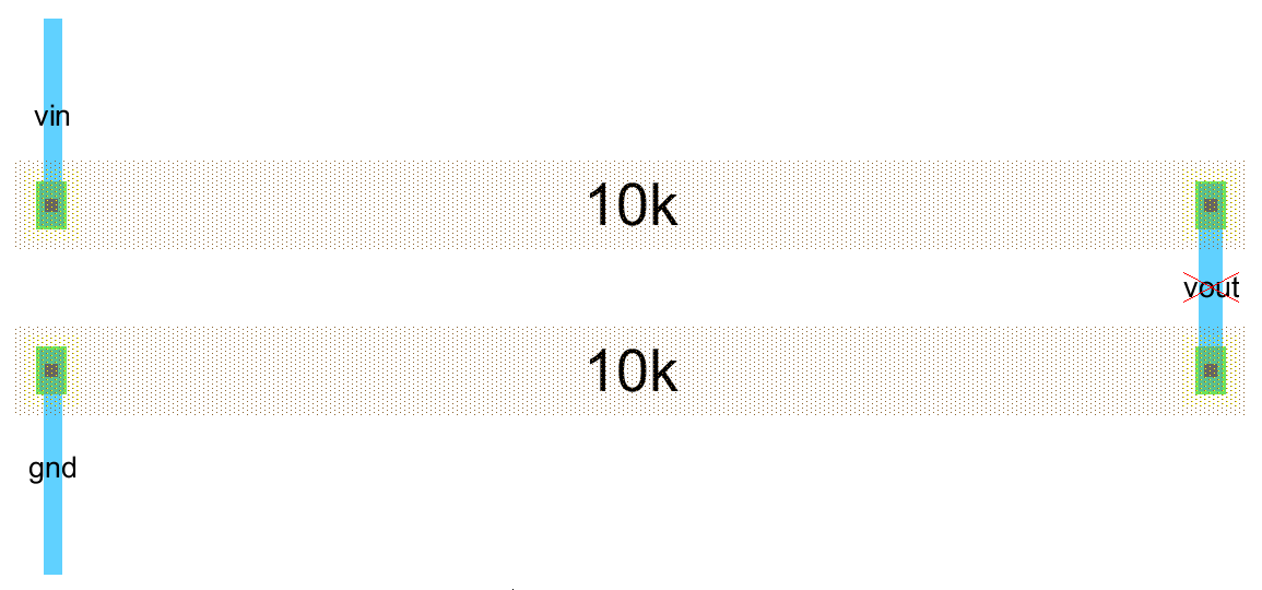
Next, just like we did in the schematic, let’s label the Arcs: vin, vout, and gnd.
We can do this by going to the Arc properties (select and press Ctrl+I), and change the Name. If you find the text appear on the Arc is very small, then just clik Props. next to Name in Arc Properties. A Text Properties window would pop-up. Change the Text Size to 5 or more (depending on the text size you want).
You can reach to Text Properties in another way as well. The following figure (i) shows the small labels of the Arcs in the circles.
Zoom in around the Arc name and select the text as seen in figure (ii).
Using Ctrl+click may be very useful here.
The click Ctrl+I to reach Text Properties.
The following figure shows the Resistive_divider layout with visible labes.
Run DRC to check the design is free of error or not.
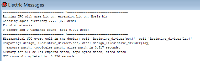
This layout cell should match the schematic cell. Verify this by running the NCC (aka LVS check).
The following figure shows the Electric Messages for DRC of layout and NCC of both layout and schematic (LVS).
Note that the names of the Arcs don’t have to match for the cells to pass NCC. The Arc names are useful for humans but don’t affect circuit operation.