The main steps in ASIC physical design flow are:
- Design Netlist (after Synthesis)
- Floorplanning
- Partitioning
- Placement
- Clock-Tree Synthesis (CTS)
- Routing
- Physical Verification
- GDS II Generation
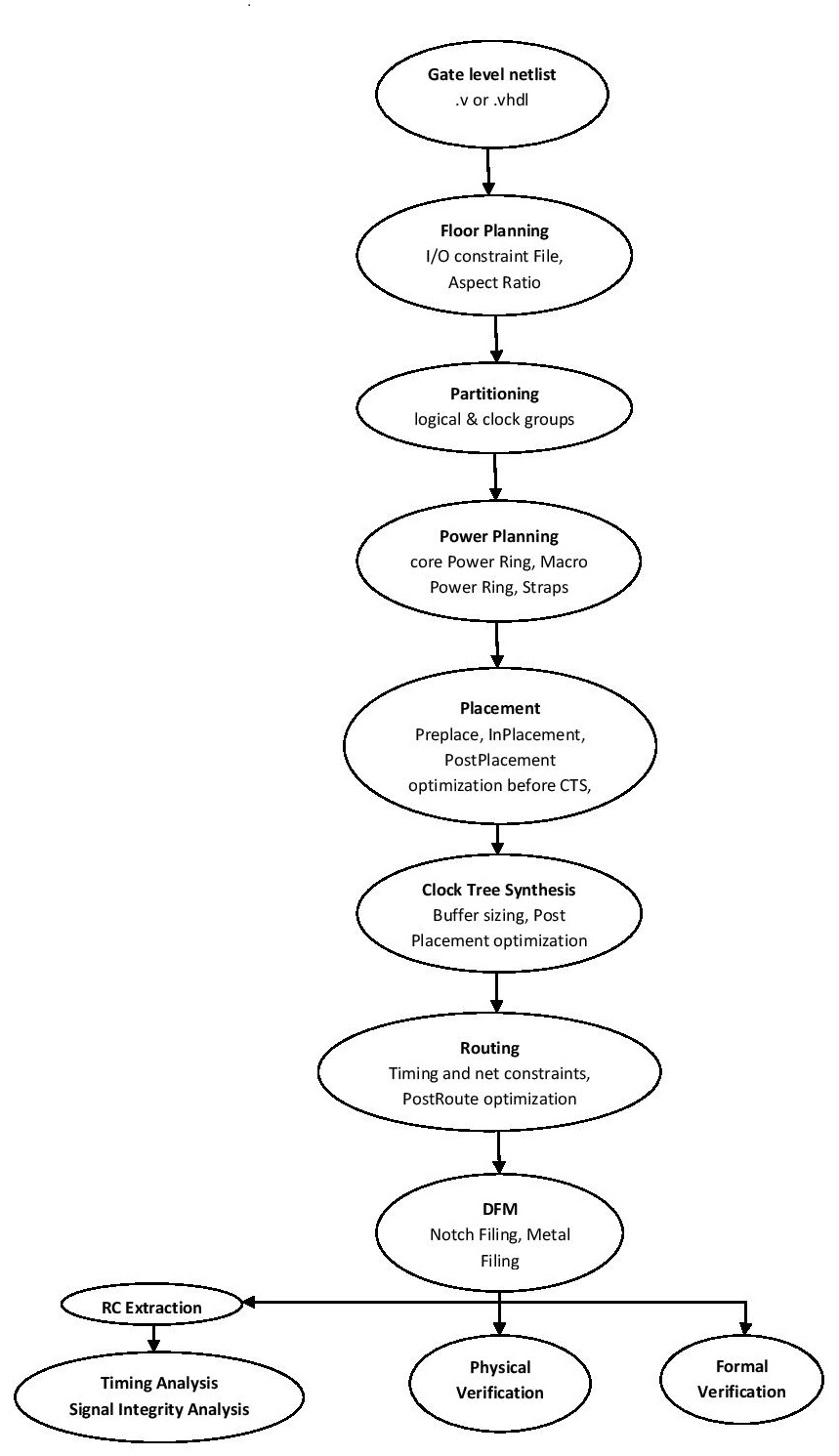
These steps are just the basic. A more detailed design flow is presented in the picture below:
The ASIC physical design flow uses the technology libraries that are provided by the fabrication houses. Technologies are commonly classified on the basis of minimal feature size. The basic sizes available are 2µm, 1 µm, 0.5 µm, 90nm, 45nm, 18nm, 14nm, etc. They may also be classified according to the manufacturing process like: n-well process, twin well process, SOI process etc.
The steps of ASIC design flow are explained below:
DESIGN NETLIST: Physical Design is based on a netlist which is the end result of Synthesis process. The netlist contains information on the cells used, their interconnections, area, and other details. Synthesis tools that are used are:
- Cadence RTL Compiler/Build Gates
- Synopsys Design Compiler
During the synthesis process, all the constraints are applied to ensure the design meets the functionality and speed. Once the timing and functionality is verified, it is sent for physical design flow.
PHYSICAL DESIGN STEPS:
1. FLOOR-PLANNING: The first step in physical design is floor planning. In this process, the structures are identified which should be placed together meeting the performance and timing requirements. The desire to have everything close to everything else is followed. But based on the area and hierarchy, a suitable floor plan is decided. Floor planning is defined as taking account of macros used in the design, memory, other IP cores and their placement needs, the routing possibilities and also the area of the entire design. Area and Speed are two factors which can be trade off against one another. Optimizing the design for minimum area allows the design to use fewer resource and thus increasing the speed of the system.
As a general rule, data-path benefit most from floor planning, and other logics like state machines, or some random logic are placed to the left section of the place and route software.
2. PARTITIONING: It is a process of dividing the chips into small blocks. This is done mainly to separate functional block and also to make placement and route easier. Partitioning can be done in the designing phase as the design engineer usually divides the whole system to sub-blocks and then proceeds to design each module. These sub modules/blocks are later connected in TOP LEVEL module.
3. PLACEMENT: Before the placement, all Wire Load Models(WLM) are removed. Placement uses RC values from Virtual Route(VR) to calculate timing.
Placement can be done in four phases:
I. Pre-placement optimization: In this process optimization happens before netlist is placed. In this process high-fan out nets are collapsed downsizing the cells.
II. In placement optimization: In this process logic is re-optimized according to the VR. Cell bypassing, cell moving, gate duplication, buffer insertion, etc. can be performed in this step.
III. Post Placement optimization: Netlist is optimized with ideal clocks before CTS. It can fix setup, hold violations. Optimization is done based on global routing.
IV. Post placement optimization after CTS optimization: Optimization is performed after the CTS optimization is done using propagated clock. It tries to preserve the clock skew.
4. CLOCK TREE SYNTHESIS (CTS):
I. Ideal clock before CTS: The goal of CTS is to minimize the skew and insertion delay. Clock is not propagated before CTS. If clock is divided the separate skew analysis is done. Global skew achieves zero skew between two synchronous pins without considering logic relationship and local skew achieves zero skew between two synchronous pins while considering logic relationship.
If clock is skewed intenetionally to improve the setup slack then it is known as useful skew.
II. Clock After CTS: In clock tree optimization cloak can be shielded to remove noise. But shielding increases area by 12% to 15%. Optimization is achieved by gate sizing, buffer sizing, level synthesis and HFN synthesis. Hold slack is improved in optimization after CTS. As a result of CTS a lot of buffers are added.
5. ROUTING: There are two types of routing in physical design process:
I. Global Routing: In this type of routing a loose route is generated for each net with estimated values. Rough estimation of values can be done by calculating the delays for fanout of wire. Global Routing is further divided into Line Routing and Maze Routing.
II. Detailed Routing: In detailed routing the actual geometry layout of each net is calculated i.e actual delays of wire is calculated. The actual delays can be obtained by several optimizations like Timing optimization, CTS, etc.
6. PHYSICAL VERIFICATION: Physical verification checks the correctness of generated layout design. This includes:
I. DRC (Design Rule Check)
II. LVS(Layout vs. Schematic)
III. ARC (Antenna Rule Checking)
IV. ERC (Electrical Rule Checking)
7. GDS II: Graphic Database System: GDS II is a database file format which is the industry standard for data exchange of IC layout artwork. It is a binary file representing planar geometric shapes, text labels and other information about the layout in hierarchical form.
