Modern day Syetem-on-Chips are so complex that pre-silicon verification is no more the sufficient step to capture all the design bugs. Even with sophisticated verification process, achieving 100% coverage is difficult. Due to this, few bugs escape from the pre-silicon verification till the actual product on silicon. So, now-a-days industries perform post-silicon validation (commonly known as post-silicon debug) as a mandatory verification step on few initial pre-production chips before mass production.
Read Pre-Silicon Verification vs. Post-Silicon Validation
Objectives:
- To capture the escaped design bugs from pre-silicon verification
- To test the power-on of the newly designed chip
- To check the functionality of the chip in real environmental scenarios
Advantages:
- Runs at the system clock speed (in GHz range), while the pre-silicon verification runs at simulator speed (in MHz range). So faster verification.
- Checks the validity of the design in real environmental scenarios
Challenges:
- Very low observability and controllability on system internal states, as only input and output pins on a real silicon chip can be controlled or observed. Whereas any internal signal can be observed in a simulator during pre-silicon verification.
Requirement:
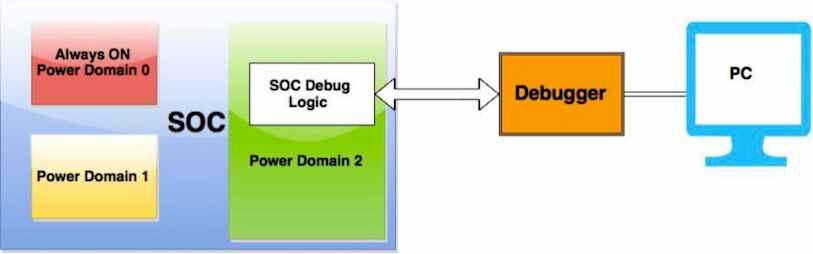
- Efficient design-for-debug (DfD) structures are required to be employed during product design phase, which would provide required infrastructure for system validation during post-silicon validation step.
Major components of DfD structure and their working will be discussed in an upcoming article.