MPW stands for Multi-Project Wafer, which is a cost-effective way to prototype integrated circuits. In an MPW, multiple projects share a single wafer during the fabrication process, which enables lower costs by spreading the cost of the wafer among multiple projects. Typically, several customers with small designs collaborate to share the costs of the wafer and the masks, which are the patterned plates used to transfer the design onto the wafer. MPWs are often used for proof-of-concept prototypes or for low-volume production. MPW services are typically provided by foundries, which offer a variety of technologies, foundry processes, and options for design and layout. By using MPWs, designers can prototype their designs more quickly and inexpensively, which helps accelerate the development of new integrated circuits.
The above paragraph provides a summarized brief on MPW in VLSI. To gain more understanding of MPW, please read the rest of the article.
VLSI, or Very Large Scale Integration, is a critical technology that has enabled the modern-day electronics revolution. In VLSI design, one of the critical steps is the fabrication of integrated circuits. Multi-Project Wafer (MPW) service is a cost-effective solution for this process. MPW refers to the sharing of a single wafer for the fabrication of multiple integrated circuits. In this article, we will explore MPW in VLSI, and its benefits.
What is MPW in VLSI?
MPW in VLSI refers to a shared wafer service that allows multiple customers to share a single wafer for the fabrication of their integrated circuits. In MPW, multiple customers can take advantage of a single wafer run, thus reducing their fabrication costs. MPW is an economical solution for low to medium-volume IC production, particularly for prototypes, pilot projects, and early-stage product development. This approach is especially useful for smaller companies, startups, or designs that need only a small number of chips, as the cost of a full wafer fabrication run can be quite high.
For example, consider an MPW service provider who has a capacity of 100 chips per wafer. Rather than each customer ordering a full wafer run of 100 chips, they can each order a smaller quantity of chips to be fabricated on the same wafer. This allows the service provider to allocate the available wafer space more efficiently, as well as offer lower costs to individual customers.
The MPW process usually requires the customer to provide their design files to the service provider, who then masks and fabricates the chips on the common wafer. The customer then receives the fabricated chips, which can be tested and packaged for use in their final application.
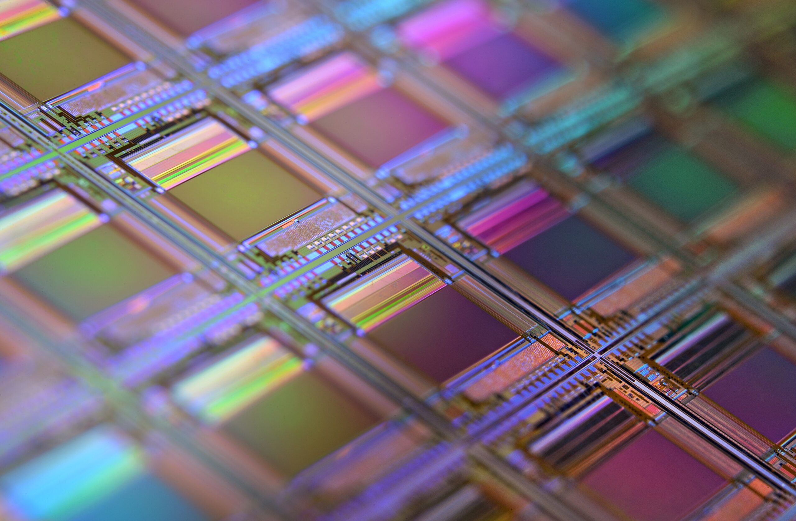
A zoomed-in image of a silicon wafer
Benefits of MPW in VLSI
MPW in VLSI offers several benefits, including:
-
Reduced Costs: One of the primary benefits of MPW is that it reduces the cost of IC fabrication. By sharing a single wafer, multiple customers can split the cost of the fabrication process, resulting in reduced costs.
-
Reduced Time to Market: MPW can significantly reduce the time to market for integrated circuits. Since multiple customers are sharing a single wafer, the wafer fabrication process is completed much faster, which leads to a reduced time to market.
-
Improved Access to Cutting-Edge Technologies: MPW provides access to cutting-edge technologies and process nodes, which would otherwise be unavailable to smaller companies.
-
Improved Resource Utilization: MPW improves resource utilization by allowing multiple customers to share a single wafer. This results in improved utilization of wafer fabrication resources, which leads to reduced costs.
Overall, MPW in VLSI provides a cost-effective solution for customers to get their chip designs fabricated while also providing a business opportunity for service providers to offer a shared wafer service. MPW services provide an opportunity for small companies or individuals to have their integrated circuits fabricated without having to bear the high cost of a full wafer fabrication run.