This post illustrates the circuit design of Even Parity Generator. State Machine diagram for the same Parity Generator has been shown below. Click here to realize how we reach to the following state transition diagram.
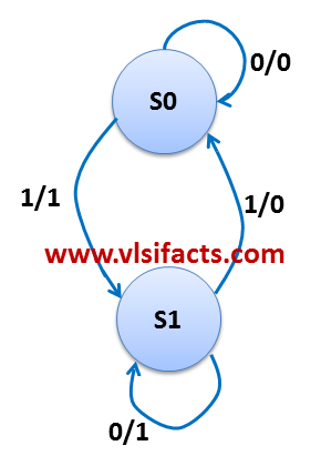
Mealy Machine for Even Parity Generator
Click here to learn the step by step procedure of “How to synthesize a state machine / How to boil down a state machine to the circuit level”.
Now as we have the state machine with us, the next step is to encode the states. For 2 states:
State Encoding
S0 0
S1 1
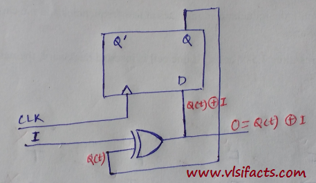
We need only 1 flipflop to represent these 2 states. For this example we will be using D flipflip to design the circuit.
Let’s draw the state transition table using the Excitation table of D flipflop
| PS
Q(t) |
I
Input |
NS
Q(t+1) |
Excite
D |
O
Output |
| 0 | 0 | 0 | 0 | 0 |
| 0 | 1 | 1 | 1 | 1 |
| 1 | 0 | 1 | 1 | 1 |
| 1 | 1 | 0 | 0 | 0 |
Now to realize the combinational logic, we have to find out the Boolean expression for 2 output variables (of the above table) D and O in terms of 2 input variables Q(t), and I.
If we would notice the column of “D” and “O” then we would find both are same and represents the output column of a XOR gate.
D = Q(t) ⊕ I
O = Q(t) ⊕ I
Let’s draw the respective circuit diagram for the even Parity Generator.
1 comment for “Circuit Design of Parity Generator”