Setup and Hold time concept is one of the fundamental concepts that is very necessary for closing and analysing and timing margin. The analysis in digital domain, in Reg to Reg system is very popular but the root cause of Setup and Hold time is often not taken care of in the education system. This Post elaborates the cause of setup analysis in a single D latch taking the Transistor level schematic into account, also I will try to explain the points where Setup and Hold time is measured and why we do so and why we can not write it on any other points.
Fig.1 Displays a Transistor Level Diagram of a simple D-latch, D is the input and I1, I2 are the inverters in the data path of the latch, T1 is the forward path transmission gate and T2 is the feedback path transmission gate, while L_I_1 and L_I_2 are the cross coupled latch inverters. The latch is controlled by the signal CK.
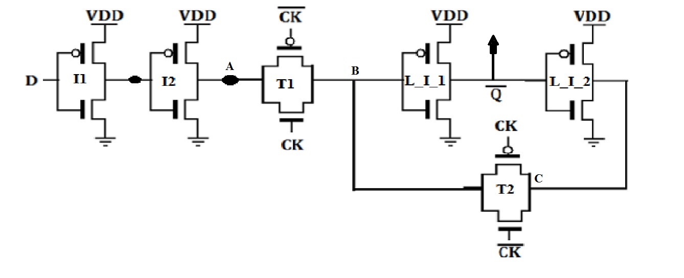
Fig.1 A single D Latch
Fig.2 shows the CK signal used, the CLK_delay is the delay between the rising edge and the falling edge of the CK and CK_bar signal.
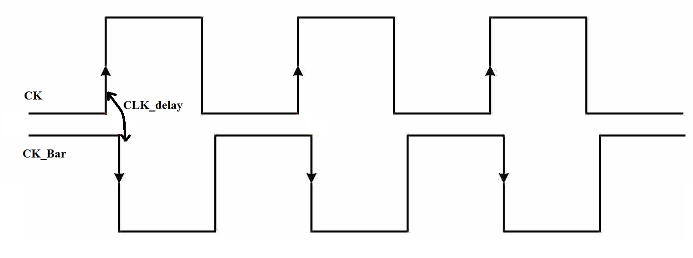
Fig.2 Clock signals used .
Setup Analysis
1. Setup time is the minimum time required for the data to get settled before the latching edge of the clock in this case it is the Rising edge.
2. The requirement of the setup time arises from the fact that the latching action is performed by the cross coupled inverters L_I_1 and L_I_2, the latch is a Bi-Stable which means that is is stable at two points either (0,1) or (1,0)., this implies that if the latch is at any between logic, it can go in either direction, so to have the safest of the operation the logic at point B should be same as the logic at point C. This means any change in data should propagate to point C before the latching action of the latch begins that is closing of the T2 and opening of T1.
3. Moreover as the first latching edge of the clock arrives in this case it is the rising edge, corresponding transistor of T1 begins switching off and T2 begins conducting, this causes the output to degrade and finally the latch is unable to sample the changed data and it latches the previous data only, which is a functionality failure.
Fig.3 and Fig.4 displays the simulation of setup violation in the D-latch , the blue line is the clock edge, the Red one is the data, which in multiple simulations is pushed near to the clock edge,and the green one is the output data which is inverted of the input data due to the circuit taken.
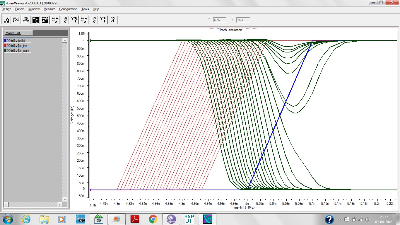
Fig.3 Setup Simulation and Violation (A)
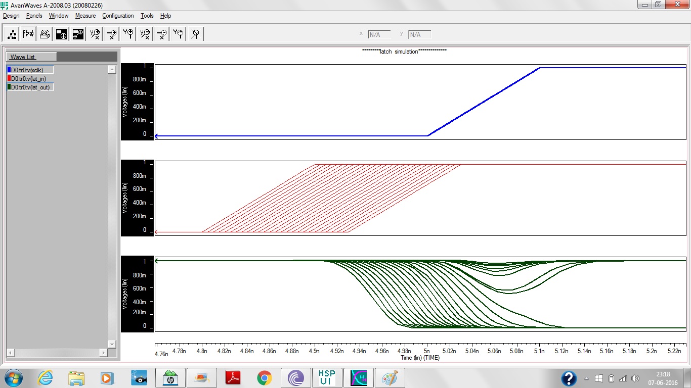
Fig.4 Setup Simulation and Violation (B)
4. As it can be clearly seen that as we push the data towards the clock edge the output data degrades and finally it tries to reach the level 0 but reverts back to the logic 1 as the latching action of the latch overcomes the changed data which was not able to propagate to point C, and the previous data which was residing at C take over the change.
5. So going by this explanation one can say that if this clock is the same as external clock then at the basic explanation we can say that the for the surest of the operation setup time is the data delay which is from the point D to C and it is commonly denoted as MAX Data delay
6. Different measurement standards calculate Setup time differently, some industry parameters measure it like the minimum time before the edge of the clock for which gets output degradation is up to 5% of the relaxed value.
For the basic understanding and explanation we can conclude that for the surety of the operation the data should reach the point C before the latching just kicks in, and this delay is the SETUP time of the latch as if some one violates it, the output data will start degrading, now its on the design requirement, that up to which extent degradation is allowed.
I hope this will suffice your queries, Keep following for the some more posts on Setup and Hold. Please post your queries in the comments or start a thread in the discussion forum.
2 comments for “SETUP Time and SETUP Violation in a Single D Latch”