MOS scaling has introduced many undesired effects, known second order ones being channel length modulation, velocity saturation, mobility degradation etc. These are introducing a new set of challenges for the designers. From the performance perspective, supply voltage scaling has reduced the driving capability of MOS due to decrease in effective overdrive voltage. On the other hand, Process has made it worse by introducing high mobility degradation which in turn has reduced the drive current of MOS. So going by the situation here, with every new node out, MOS is getting weaker and weaker. At the same time it is expected to pull off higher performance from every last generation. SEEMS TOUGH !!!
Have you ever thought how we are able to do that ????
We have a savior here and its name is “Process induced strained silicon”. Something which is actively being used in sub 100nm technologies. Seems like a process related stuff, then why we being designer should care about it. Let me explain but let’s first talk about this savior guy in very simple terms.
This is a process technique to enhance the mobility of the charge carriers of MOS. This is done through applying some high stress film across the channel during fabrication. Using the same process flow on the wafer, we apply compressive strain into P-type and tensile strain into N-type which leads to improve both electron and hole mobility. Let’s not dig deep into process related things and all the physics involved behind it. But this step, somehow, favors the holes more than electrons and hence the improvement in the hole mobility is higher than that of electrons.
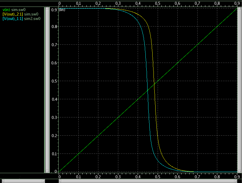
So now since we have talked about our savior, let’s see what the impact of this mobility improvement is. The first observation, obviously, is the driving capability of both NMOS and PMOS is improved. But here is the catch, the driving capability of PMOS is improved with a larger factor than of NMOS. This leads to a stronger PMOS with every coming generation. To look for the effect, we can just go on and plot the inverter characteristic for different beta-ratio (PMOS to NMOS W/L ratio) and observe inverter’s switching threshold. Needless to say, the beta-ratio which result in inverter switching threshold of Vdd/2 indicates the exact difference in strength of PMOS and NMOS for a particular technology. Following figure is the Inverter DC characteristic for beta-ratio of 2:1 and 1:1 in 16nm technology. Surprisingly, conventionally used 2:1 beta-ratio seems skewed in this case while ratio 1:1 has switching threshold of Vdd/2. So for 16nm, NMOS and PMOS are of same strength.
 Moreover, if we intend to build an inverter with the switching threshold of Vdd/2 for different technologies then the beta ratio would look something like this.
| Technology Node | Beta – ratio |
| 65nm | 2.1:1 |
| 40nm | 1.66:1 |
| 28nm | 1.3:1 |
| 16nm | 1:1 |
| 7nm | 0.9:1 |
Just look at the beta-ratio of 7nm column, it says that for an inverter of Vdd/2 switching threshold, the PMOS size will be smaller than NMOS. Now this is contrary to what we have been taught in the books and class. In previous generations PMOS device was made of higher size so as to compensate the mobility imbalance, occupying the lager area. But now PMOS is no longer the culprit!!!
Reference: http://bitsonchips.com/references/ref29.pdf
Contributed by: Jitendra Yadav