The Electronics engineers should know the steps to design a particular circuit. While we study, we directly study the properties of the electronic block and the circuit diagram of the corresponding block. We never think how had we landed up to that particular circuit diagram. For example when we talk about digital Multiplexer, Decoder or Counters; we directly find the block diagrams and the circuit diagrams of these modules. And we never think about the design process. So, in interviews, students fail to design a simple combinational logic. Though this post seems to be a simple one, and few may find nothing new is here; but I thought of posting this as it would help the newbies and also to them who wand to revisit the concept of designing a combinational circuit.
Steps to be Followed:
-
Understand the problem statement (realize how the outputs of the circuit depend on the inputs to the circuit)
-
Draw the Truth Table (Truth Table establishes the relationship between the outputs and inputs for all the possible input combinations)
-
Derive the minimized Boolean Expressions for the outputs w.r.t. the inputs (You can use the K-Map method)
-
From the Boolean expressions draw the logic circuit
In this post, we have considered a very simple problem to explain the above 4 steps:
Design Problem: Design a 3 input, 1 output digital logic circuit which will take all the octal digits (0, 1, … 7) as its input and produce the even parity bit for the corresponding octal digit.
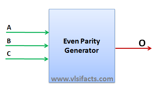
Even Parity Generator Block Diagram
Step 1: The circuit has 3 inputs (as the octal digits need 3 bits to be represented) where it would only take the octal digits. The output would generate the even parity bit for the corresponding input given. For example if the input is octal digit “2” i.e, in binary “010”; the generated parity bit would be “1”. Click here to understand the even/odd parity bit generation concept.
Step 2: Let’s draw the truth table for the design
| A | B | C | O |
| 0 | 0 | 0 | 0 |
| 0 | 0 | 1 | 1 |
| 0 | 1 | 0 | 1 |
| 0 | 1 | 1 | 0 |
| 1 | 0 | 0 | 1 |
| 1 | 0 | 1 | 0 |
| 1 | 1 | 0 | 0 |
| 1 | 1 | 1 | 1 |
Step 3: Let’s draw the K-map for the above truth table and find the equivalent Boolean expression.
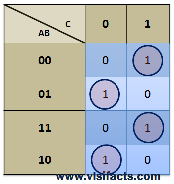
K-Map for Even Parity Generator of Octal Digits
As we can see that there is no minimization possible; the final Boolean expression would be:
O = A’B’C + A’BC’ + AB’C’ +ABC
Step 4: Now as we have the Boolean Expression with us, we can draw the logic circuit for the same:
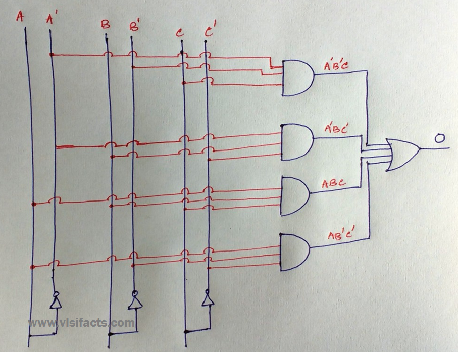
Even Parity Generator Circuit
Hope you have learned a very basic design procedure. Stay tuned to VLSIFacts to get more updates like this.
2 comments for “Step by Step Method to Design a Combinational Circuit”